DLTS (Deep Level Transient Spectroscopy)
About the DLTS method
The DLTS method was developed by Lang in 1974 and has undergone several improvements since then.
Here we will first describe Lang's approach in detail as the 'conventional' or 'traditional' DLTS method, and then briefly touch on the evolution of the technology to the present day.
DLTS (Deep Level Transient Spectroscopy) Method
The characteristics of semiconductor materials are greatly affected by minute internal impurities and lattice defects (crystal defects), making their evaluation extremely important.
The DLTS method is an excellent technique for the highly sensitive detection of the electronic states (deep levels) caused by these crystal defects, and has been widely used since its development in 1974 by Lang at Bell Labs in the United States.
Due to its measurement principle, DLTS requires samples with semiconductor junctions (such as Schottky or pn junctions). The dynamic process of carriers (such as electrons) trapped in deep levels being emitted into the band (conduction band) is monitored by the transient change in the junction capacitance of the sample, allowing evaluation of parameters such as energy level, capture cross-section, concentration, and spatial distribution.

In addition to measuring discrete levels created by single atomic defects, DLTS is also effective for evaluating interface states in MOS structures and continuous levels in amorphous semiconductors.
Another feature of the DLTS method is its excellent sensitivity.
While the detection limit of impurity atoms in SIMS, a well-known high-sensitivity surface analysis method, is around 10¹⁴atoms/cm³, DLTS can detect an amazingly low concentration of 10⁹atoms/cm³ or even less, depending on the conditions.
(For more details on the DLTS method, please refer to another section).
This section describes the basic principles of transient spectroscopy methods such as DLTS and ICTS.
Both DLTS/ICTS methods share the same basic measurement principle of monitoring deep level carrier emission processes through transient changes in the junction capacitance of a sample.
Therefore, unless specifically compared or contrasted, the two methods will be referred to collectively as DLTS.
Measurement Samples
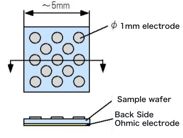
Due to its measurement principle, DLTS requires samples with semiconductor junctions (Schottky, pn or MIS structures).
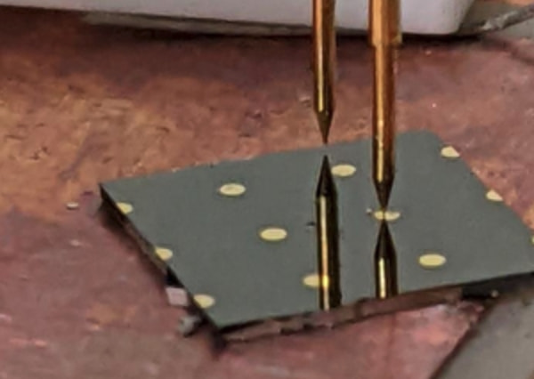
For example, to evaluate deep levels in bulk semiconductor materials, a Schottky junction is created by depositing a metal electrode on the front surface and an ohmic electrode on the back surface, resulting in a sample with a Schottky diode structure.
If the sample is a device that already has a diode structure, it can be used directly for measurement.

Measurement Principle
The basic measurement principle — demonstrated here with an n-type Schottky junction — also applies to pn junctions and MIS structures.
Click here to download a detailed explanation of the principle.
Features of the DLTS Measurement Service
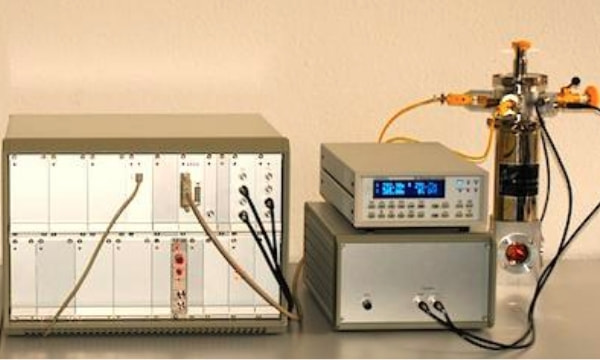
Ceramic Forum provides DLTS measurement services. DLTS is a powerful technique for detecting and evaluating deep level traps caused by heavy metal impurity atoms and crystal defects in semiconductor materials.

-
Highly sensitive detection of impurities and defects
Detects impurities and defects in semiconductor materials with high sensitivity.
Ideal for evaluating crystal quality.
-
Advanced technology and equipment
Measurements are carried out accurately and quickly using the latest DLTS equipment.
Specialized technicians perform the measurements and provide highly reliable data.
-
Wide material compatibility
Applicable to all types of semiconductor materials including Si, GaAs, SiC, GaN, and diamond.
-
Data analysis and reporting
Detailed analysis of measurement results is provided in easy-to-understand reports.
Data reliability and reproducibility are guaranteed.
Ceramic Forum’s DLTS measurement service provides strong support for semiconductor R&D. For more information or service requests, please contact us.


