Crystalline Diagnostic System (CS2, CP1)
made Crystalline Tester 🄬 CS2,CP1
Crystalline Tester CS2 (Macro Diagnostics)
Crystalline Tester 🄬 The Crystalline Tester CS2 is a non-destructive, high-speed diagnostic tool for evaluating the macroscopic crystallinity of n-type SiC wafers.
After wafer setup, the system performs fully automated transmission polarization measurements, image analysis and numerical analysis to generate a diagnostic report.
Key features
-
Fully automated diagnosis
Automated scanning and imaging
Automatically switches between cross-polarized and parallel-polarized transmission imaging across the wafer at 20 µm/pixel resolution and performs image processing for diagnosis.
Physical property analysis
Numerical analysis of all pixels in polarization measurements quantifies nitrogen concentration distribution, macro defect distribution and residual strain in the wafer.
Diagnostic report generation
An Excel file is automatically generated as a diagnostic report.
The Excel file integrates various processed images and physical property diagnostic results.Utility
Operates on just AC100V (1.5kVA) and requires no warm-up, enabling quick use during research or manufacturing operations.
-
High-speed diagnostics
Scanning, analysis and diagnostic reporting:
8-inch wafer: 150 seconds
6-inch wafer: 110 seconds
4-inch wafer: 90 seconds


3D-MAP showing the distribution of nitrogen (n-type impurity) concentration in the crystal, showing the segregation of N into faceted regions during SiC substrate crystal growth.

Binarized analysis results showing automatic classification of local birefringence images induced by internal crystal defects.

3D-MAP visualizing local strain distribution caused by internal defects, overlaid on the residual strain across the entire wafer.
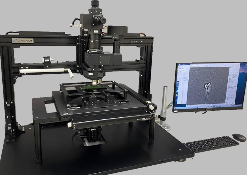
Crystalline Tester CP1 (Micro Diagnosis)
Crystalline Tester 🄬 CP1 provides non-destructive 3D diagnosis of threading dislocations and inclusions in wafers, as well as carrot and triangle defects in epi layers.
Measuring system optics
This system is the first application of phase contrast microscopy, commonly used in biotechnology, to semiconductor wafer inspection. It enables three-dimensional diagnosis of micro-defects such as threading dislocations (TED, TSD, TMD, MP), inclusions and extended epilayer defects (carrot, triangle) in wide bandgap semiconductors such as SiC, GaN and AlN.
Main Features
-
High-resolution Diagnosis
High-resolution observation of dislocations
Phase contrast microscopy detects the refractive index modulation due to the inelastic stress field near the dislocation core, allowing closely spaced dislocations to be observed without interference. Observation of threading dislocations is possible at a dislocation density of 10⁷ cm-².
-
Versatile crystal diagnostics
Identification of TED/TSD/MP in SiC epi-layers
Automatically identifies TED, TSD and MP in SiC epi-layers, extracts coordinates and performs calculations. (See Figure 1)
Diagnosis of Dislocation Core Tilting
As shown in Figure 2, even for TSDs within the same 10 mm thick SiC epi layer, depth profile changes associated with dislocation core tilting can be observed for different growth rates.
Dislocation Depth Profiling
Figure 3 shows an example of epi layer depth profiling. Tracing the transversely segmented defects from the surface of the fast grown SiC epi layer in Figure 2 to the epi/substrate interface confirms that one is associated with the substrate TSD and the other is not caused by a substrate dislocation.
Observation of polarized phase contrast images
When observing phase contrast images of threaded dislocations, the polarization orientation selectivity of the phase contrast is observed by superimposing the polarization effect on the optical system. This allows us to examine the relationship between the Burgers vectors of each dislocation and the possibility of a detailed classification of each dislocation (see Figure 4).
Fast and easy operation
LED light source, automatic XYZ control stage, auto-focus control, automatic image processing software and Excel output of results make wafer diagnostic operations easy to perform.
Utility
Operates on AC100V (1.5kVA) only and requires no warm-up, allowing quick use during research and manufacturing operations.


