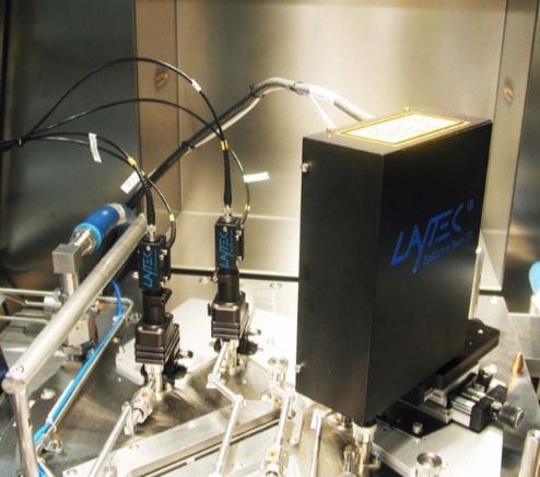
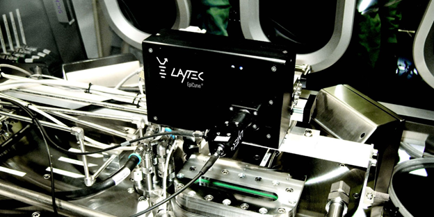
LayTec in-situ Measurement System
Product Overview
This system measures with extremely high precision film growth rate, film thickness, substrate warpage, wafer surface temperature, and other parameters during epitaxial growth processes using various film growth systems such as MOCVD and MBE.
It is also compatible with nanoscale structures.
In film growth processes for various materials such as GaN, the actual wafer surface temperature is considered to be the most important film growth condition, and this system measures temperature in real time with an accuracy of ±1K.
High-end models are capable of a wider range of measurements and analyses.
It is also compatible with multi-wafer susceptors, allowing selective measurements for each wafer.

Product Features
1.Real-time Monitoring
Compatible with deposition equipment such as MOCVD and MBE, measuring deposition rate, film thickness, substrate curvature, and wafer surface temperature in real time.
Achieves temperature measurement accuracy of ±1K, supporting the optimization of deposition conditions.
2.Compatibility with Various Materials
Supports the deposition processes of wide-gap semiconductor materials like GaN, SiC, and AlN./p>
Enhances the accuracy of deposition processes by measuring the actual temperature of the wafer surface in real time.
3.Mapping System
Conducts mapping of wafer-wide reflectance, film thickness distribution, substrate curvature, sheet resistance, and transmittance.
Capable of measuring multiple wafers simultaneously, improving production efficiency.
4.Advanced Analysis Capabilities
Automated analysis of Dip wavelength position and Stop-band width during the deposition process.
Provides wafer mapping systems linked with measurement data obtained from in-situ devices.
Technical Specifications
Temperature Measurement Accuracy: ±1K
Compatible Equipment: MOCVD equipment, MBE equipment, etc.
Compatible Materials: GaN, SiC, AlN

Manufacturer Information

LayTec AG (Germany)
Founded in 1999, LayTec is a leading company in the field of in-situ epitaxial sensors.
Selected as one of the 50 fastest-growing technology companies in Germany for three consecutive years from 2009.
Currently, over 2500 measurement systems installed worldwide, with 75% in Asia, 10% in North America, and 15% in Europe.


