
SemiconductorSemiconductor


GlassGlass


Ceramic Forum's Goals
Our company is committed to bridging advanced technologies across borders,
empowering innovation in the semiconductor and glass industries. We aim to be a trusted
partner for both overseas manufacturers entering the Japanese market and Japanese
suppliers expanding globally.
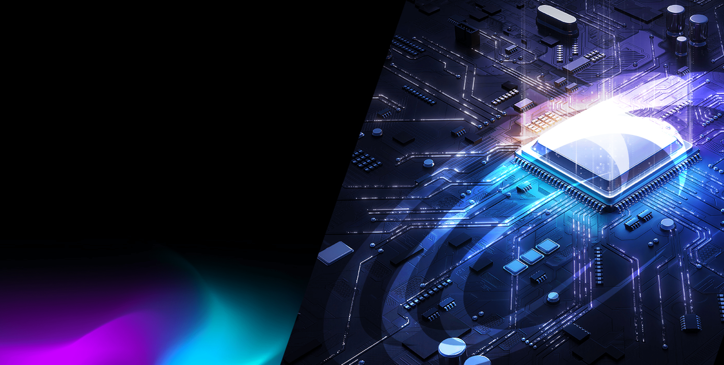
Wide Bandgap Semiconductor
SiC Wafers, GaN Wafers,
DLTS Measurement Equipment, etc.
Glass Manufacturing Technology
Precision Molding Simulation,
Glass Melting, etc.

Technical Sales will select the best technology and products for customers.


Importing the latest technology from
our international partner companies

Wide Bandgap Semiconductors
Wide Bandgap Semiconductors
Wide Bandgap Semiconductors
Wide-Band-Gap Semiconductor
-
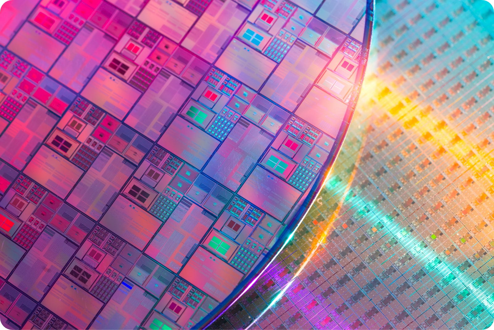
What Are Wide Bandgap Semiconductors?
Wide Bandgap (WBG) Semiconductors are materials with a wider energy bandgap than conventional semiconductors like silicon (Si) or gallium arsenide (GaAs). Thanks to properties such as high breakdown voltage, high electron saturation velocity, and excellent thermal conductivity, WBG semiconductors enable the development of high-voltage, high-frequency, and high-power devices that traditional materials cannot support.
These advanced materials are seen as key enablers for technologies that contribute to energy efficiency and environmental sustainability — including electric vehicles, LEDs, solar cells, and smart grids. As a result, WBG semiconductors are attracting growing global attention.
However, producing high-quality crystals for these semiconductors remains a challenge. Materials range from silicon carbide (SiC), which is already in mass production, to diamond, which is still in the research and development stage.
-
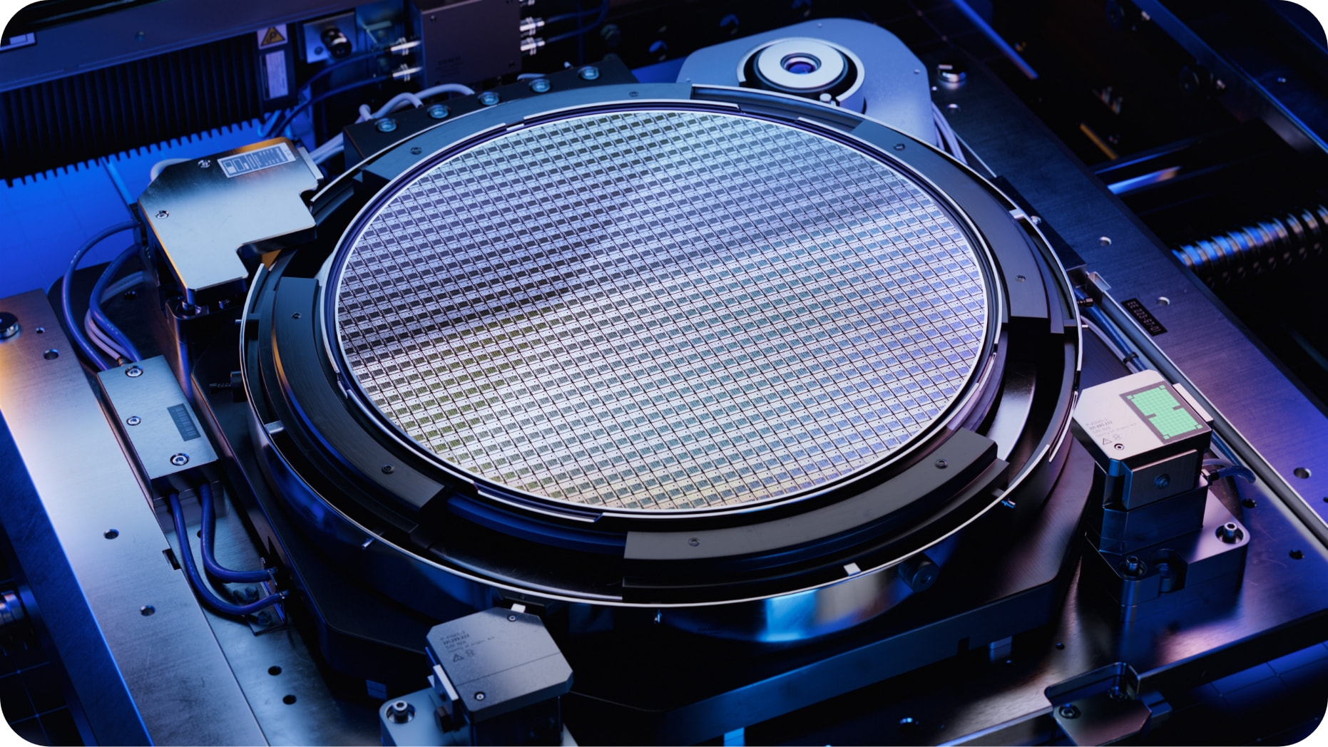
Our Wide Bandgap Semiconductor Solutions
Ceramic Forum’s Semiconductor Department provides a wide range of products and services to support the development and application of Wide Bandgap (WBG) Semiconductors — a class of next-generation materials known for their superior performance in high-voltage, high-frequency, and high-efficiency applications.
While WBG semiconductors hold enormous promise, producing high-quality crystals remains a technical challenge. Materials such as silicon carbide (SiC) are already in mass production, while others, like diamond, are still in the research and development stage.
WBG semiconductors are gaining global attention as key components in technologies aimed at energy conservation and reducing CO2 emissions — including electric vehicles, LEDs, solar power, and smart energy infrastructure. At Ceramic Forum, we are committed to providing the technologies and support needed to bring these innovations to market.
-
About Glass Manufacturing Technology
Although overall production in Japan’s glass industry has declined, demand is increasing for new infrastructure-related glass materials, including:
- • Display and optical high-tech glass
- • Architectural glass in developing countries (e.g. plate glass, bottle glass, fiberglass)
- • Safety and environmental glass (e.g. double-glazed glass for insulation)
- • Base materials for renewable energy solutions, such as solar and wind power
Focus on Glass Melting Technology
In particular, we are focused on advancing glass melting technologies to address both energy efficiency and environmental challenges. Our core objective is to deliver high-quality, energy-saving solutions for the glass manufacturing process.
Ceramic Forum offers a comprehensive, three-step solution in partnership with leading European firms:
Contact Glass Department- 1. Glass Simulation
- 2. Glass Product Analysis
- 3. Glass Melting Engineering
By integrating these processes, we help clients improve performance, reduce costs, and meet environmental goals across the entire glass production lifecycle.