
Sandia National Laboratories Orders LayTec’s EpiX Wafer Mapping System
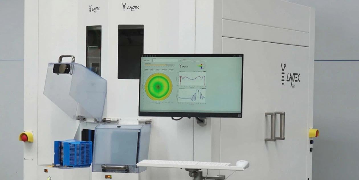
Sandia National Laboratories in the United States has ordered LayTec’s EpiX wafer mapping system for the optical characterization of advanced semiconductor materials.
The ordered system features a manual-loading configuration customized specifically for research and development applications. By combining White Light Reflectance (WLR) and Photoluminescence (PL) measurements, it enables non-contact evaluation of optical properties across the entire wafer surface.
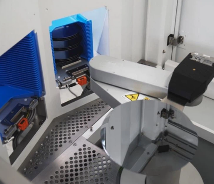
[Key Features and Applications of EpiX]
- Wide Range of Applications: Optimized for the UV-visible range, the system will support research on AlGaN-based power devices, high-frequency devices, optoelectronic devices, and emerging semiconductor materials.
- Detailed 2D Mapping: It provides two-dimensional mapping of in-plane distributions in optical and emission properties related to layer thickness and composition.
- Evaluation of Complex Structures: It enables detailed evaluation of wafer-scale uniformity and local variations, even in complex device structures such as High Electron Mobility Transistors (HEMTs).
- Flexible Modular System: Measurement modules, wavelength ranges, and wafer-loading methods can be configured according to specific requirements, supporting applications from compound-semiconductor research and development to quality control in manufacturing processes.
Ceramic Forum distributes products from Germany-based LayTec AG, including the EpiX wafer mapper and in-situ monitoring systems for MOCVD and MBE growth processes.
We propose system configurations tailored to specific applications and measurement requirements for wafer characterization and deposition-process control, with a focus on wide-bandgap semiconductors such as GaN, AlGaN, SiC, and AlN. For inquiries regarding EpiX specifications, measurement modules, supported wafer sizes, or customization options, please contact Ceramic Forum.

Related Links

