HPHT Diamond
Key Features
• Type IIa single crystal diamond substrate
• Boron concentration: 20 ppb or less
• Nitrogen concentration: 5-10 ppb or less
• Dislocation density: 10¹-10³ cm⁻² (lowest in monosector)
• High crystallinity and surface quality
• Working surface free of defects, cracks and chips (inspected under 50x microscope)
• Surface roughness Ra: 0.5-2 nm (CMP polishing available)
• Sizes up to 15 x 15 mm available
• Monosector or multisector structure
• Orientation: (100), (111), (110)
• Custom miscuts available (±0.5°)
Applications
• Quantum sensors/quantum information processing
• Ultra-high purity substrates ideal for NV center formation
• Laser/X-ray optics
• Windows and lenses for high-power lasers
• Semiconductor heat dissipation substrates
• Thermal management for GaN/SiC devices
• CVD diamond growth seeds
• Highly reproducible growth bases with surface orientation precision and miscut control
• High pressure physics research (diamond anvil cells, etc.)
Quality control system
FTDiam uses the following advanced evaluation techniques to guarantee the quality of all products:
• Diamond view analysis
• White X-ray topography
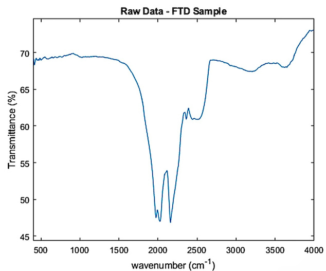
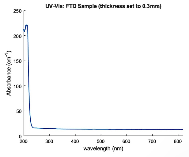
• FTIR and UV-VIS spectroscopy
• Raman spectroscopy (to confirm removal of amorphous carbon and graphite components)
• AFM surface roughness measurement
• Miscut angle evaluation by X-ray diffraction
• Distortion and residual stress analysis by polarizing microscope
Manufacturer information
FTDiam Inc.
FTDiam Inc. (Flawless Technical Diamonds, New York, USA) is an advanced materials manufacturer that uses its proprietary AHPHT technology to manufacture ultra-high purity single crystal diamond substrates. We provide high-quality Type IIa diamonds up to 15 x 15 mm for cutting-edge fields such as quantum devices for NV centers, laser and X-ray optics, and thermal diffusion of semiconductors. We boast excellent crystal quality with a dislocation density of 10¹ cm⁻² or less and boron and nitrogen concentrations at the ppb level.

